Automated PCB Layout Design on Android: The Future of DIY Electronics! What does pcb stand for in electronics
If you are looking for A Guide to the RF PCB Design you've visit to the right place. We have 25 Pics about A Guide to the RF PCB Design like PCB Layout design | FX PCB, PCB Layout Support - Embizon Technologies - PCB Design Services, Bangalore and also PCB Design – Riosh Technologies. Here you go:
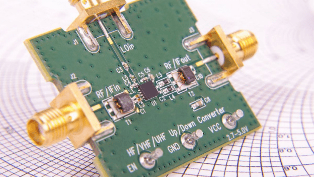
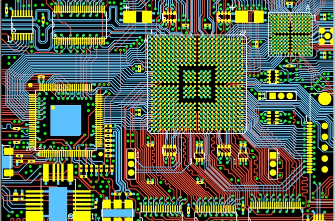
A Guide To The RF PCB Design
 hillmancurtis.com
Premium Photo | Advanced High Precision Robot Arms On Fully Automated
 www.freepik.com
Automated PCB Design Using Artificial Intelligence (AI)
 pallavaggarwal.in
pcb automated using
Top Benefits Of Automated PCB Manufacturing And Assembly - RayMing PCB
 www.raypcb.com
PCB Layout Services
 www.hytek-ed.com
pcb layout close previous next service
Automated PCB Design Using Artificial Intelligence (AI)
 pallavaggarwal.in
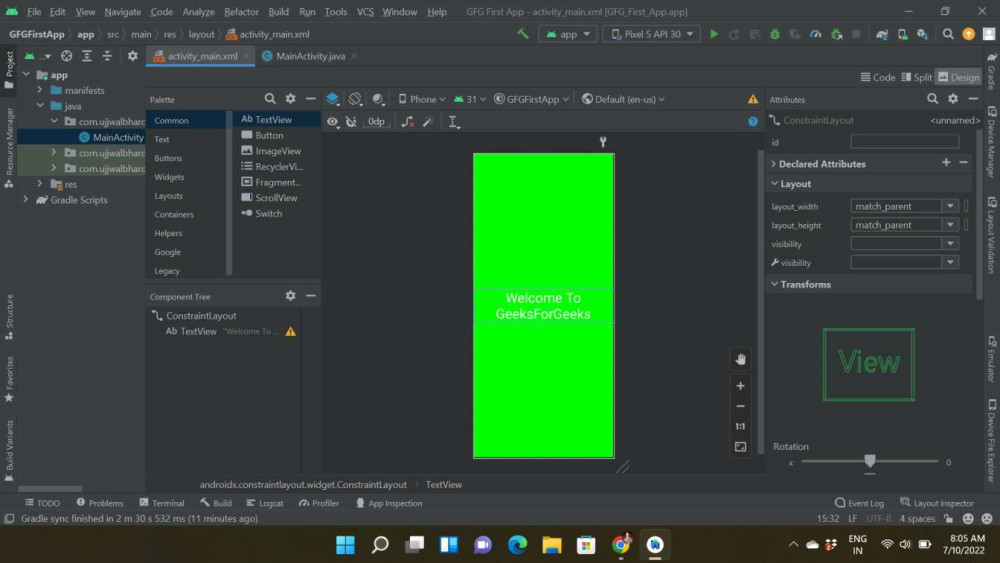
Android Layout Design Tutorial | Android UI Design Explained | Android
 ainfographie.com
A Detailed Guide To PCB Layout Design - IBE Electronics
 www.pcbaaa.com
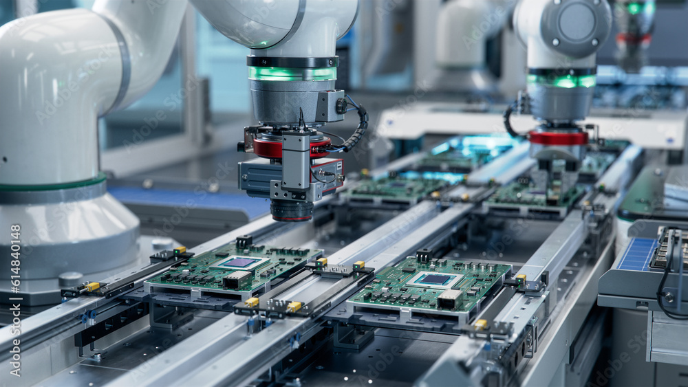
Premium Photo | Automated PCB Assembly Line With Precision Robot Arms
 www.freepik.com
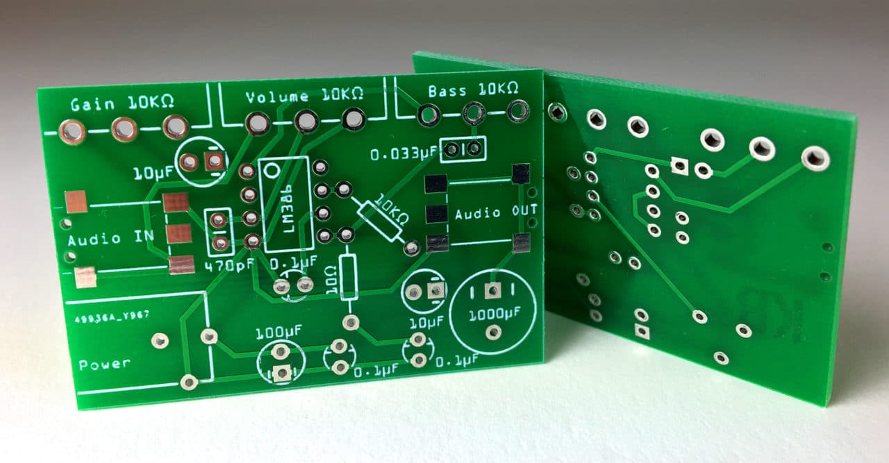
PCB Layout Design For Power Supply Circuit: Best Practices And Tips
 hillmancurtis.com
How To Design A Pcb Layout Pcb Designs - Bank2home.com
 www.bank2home.com
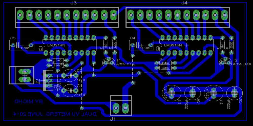
4-Layer PCB Design In KiCad 5: Quick Thoughts | Paul Bupe, Jr
 paulbupejr.com
pcb kicad
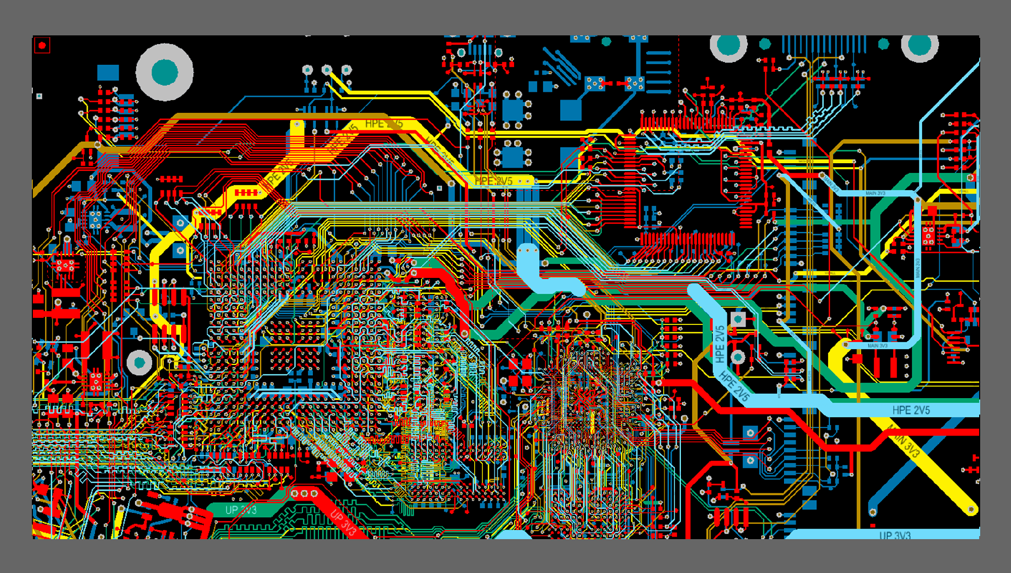
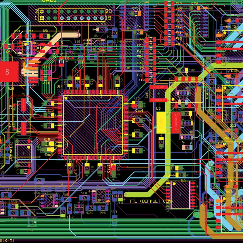
High Speed Pcb Layout Guidelines - Design Talk
 design.udlvirtual.edu.pe
PCB Design – Riosh Technologies
 www.rioshtech.com
pcb design electronics
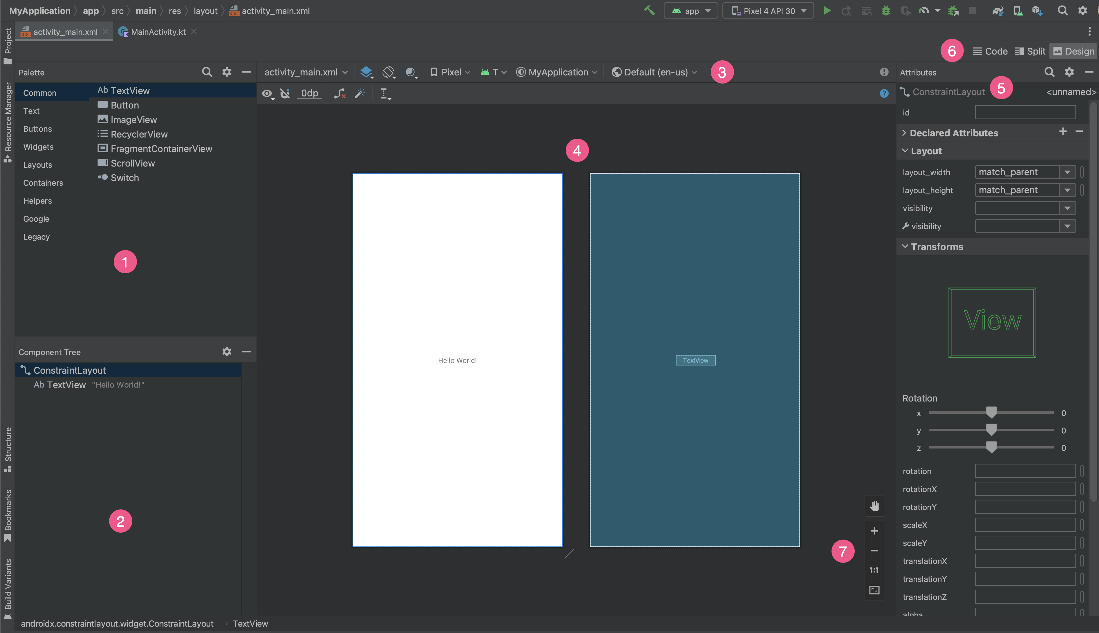
Android Dashboard/Profile UI Design Using Constraint Layout Using
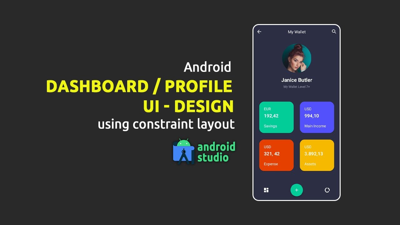 morioh.com
What Does PCB Stand For In Electronics - TechSparks
 www.tech-sparks.com
Automated Production For PCB Manufacturing - IBE Electronics
 www.pcbaaa.com
10 Most Used PCB Layout Design Tools | Sierra Circuits
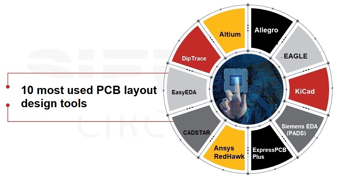 www.protoexpress.com
PCB Layout Support - Embizon Technologies - PCB Design Services, Bangalore
 www.embizon.com
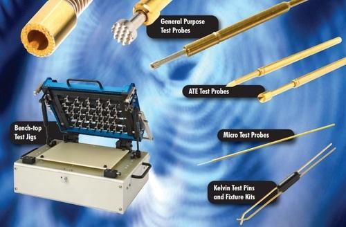
Bench Top Test Jig For PCB With PCB Test Probes
 evetechnosolutions.com
pcb jig tester automated automation probes
Android Studio Layout Design Tutorial How To Change The Size Of Icon In
 file.sejarahperang.com
PCB Layout Design | FX PCB
 sfxpcb.com
Develop A UI With Views | Android Studio | Android Developers - Thợ Sửa
 thomaygiat.com
Component Installation And Quality Control Of Circuit Board. Fully
 stock.adobe.com
PCB Function Tester (with Cyclic ON/OFF Timer)
 evetechnosolutions.com
pcb jig testing automated tester timer cyclic
Android studio layout design tutorial how to change the size of icon in. Pcb jig tester automated automation probes. How to design a pcb layout pcb designs